So many misconceptions here about DRAM. DRAM is miraculously cheap. The process probably costs about $1.50 to $2 per GB, the rest is indeed profit. That nets them maybe $4,000 per wafer - and that includes all the testing, slicing, packaging etc. An average CPU chip in your laptop is about the same size as maybe 3 DRAM chips which cost around $20.
DRAM runs on a separate process which is dominated by the difficulty of building the capacitors. These are roughly the shape of a pencil (long narrow hexagons) where the central structure which holds the capacitor needs to be etched to perfection in a process that can take days. The transistors underneath are, at that scale, about as large as the chad from a paper hole punch. The capacitors are just about as narrow as material science (limit to voltage arcing through the insulation layers) can make them so there is glacially slow progress in shrinking DRAM further. Meanwhile the transistors are at extreme limits of resolution for liquid immersion processing, as also are the lines needed to join the rows and columns. Getting those perfect requires very specialized and competent processing.
They are not easy, second rate circuits. They are a completely separate branch of the silicon world. Unfortunately since they don't scale much any more, current design methods were mature 8 years ago, the only way you get more of them is to build new factories. That means it is a seller's market in a game where building another fab costs $10B and will only succeed if staffed by really expert people. So, it is generally profitable. The 3 vendors cannot easily undercut each other since they all have roughly the same limits, and any attempt to flood the market takes 4 years to build and everyone can see it coming.
So there you are. DRAM is the pivotal technology of the current computer era. Fixing that will most likely require breakthroughs in fundamental memory technology - or a reason for demand to collapse.
>Combined with die stacking, which allows for up to 8 dies to be stacked as a single chip, then a 40 element LRDIMM can reach an effective memory capacity of 2TB. Or for the more humble unbuffered DIMM, this would mean we’ll eventually see DIMM capacities reach 128GB for your typical dual rank configuration.
So on 8 Channel 16 DIMM per socket you could fit a theoretical 32TB of memory. This is insane amount of memory and great for In-Memory Database. ( How is Intel Optane going to compete? )
This makes me wonder, what makes DRAM so expensive? It is still hovering at a median price or around $3/GB compared to NAND which is less than $0.1/GB.
The processes to form NAND and DRAM are completely different. DRAM relies on creating non-leaking capacitors which are highly difficult to manufacture at such a small scale. NAND benefits from innovations in the CPU lithography space since it's essentially all transistor based. Why would you expect them to have the same price, unless you knew nothing about the technology? Also, there are plenty of distinct competitors in the DRAM space. Do you have a source suggesting Micron and Samsung are engaging in price fixing together?
"Plenty" of distinct being Samsung, Micron and Hynix.
They are not necessarily price fixing illegally. It's just that they all keep their production and capacity expansions closely in check to not ever let prices down.
That and in rare cases when prices are down due to unexpected decline in shipments they're all very swift to shift wafers to produce something else. Feel free to dig DRAMeXchange reports for for details.
If the difficulty of DRAM is in creating capacitors at that size, why haven't we seen a shift toward SRAM (6T, for instance), which is purely transistor-based?
Sure, you have to sacrifice more transistors for the same capacity, but newer processes can fit more on the chip, right? I recall from computer architecture classes that the benefit of DRAM is the ability to use fewer transistors, but if transistors are cheap...
(I'm sure I'm missing something here. Power consumption / heat generation? I also never really understood why SRAM continues to be so expensive, when it seems like it would obviously benefit from smaller processes.)
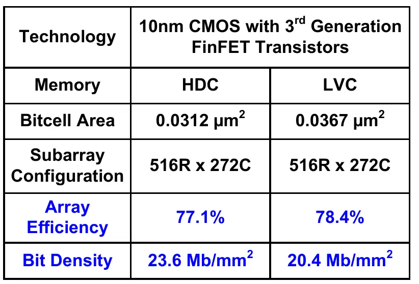
On Intel's 10 nm process you can make SRAM with a density of about 20 megabit/mm². [1] Older processes are much worse (<5 megabit/mm²). [2] A current-gen DRAM package achieves about 170 megabit/mm² (but that's two dies, probably stacked). This article [3] cites 8 Gb on 77 mm² on a 21 nm process, giving 105 megabit/mm², and 148 megabit/mm² for the DDR5 version with a die size of 54 mm². The same article shows a Samsung part with around 200 megabit/mm² density.
So even if you were to manufacture SRAM on Intel's ultra-expensive 10 nm logic process, you'd need a massive amount of silicon for the same capacity.
Totally makes sense that you wouldn't get the same capacity from the same silicon, or even close, given that SRAM uses far more transistors per cell.
But if you have issues scaling DRAM, and different scaling limits on transistor count / SRAM, it makes sense (to me at least) to start considering SRAM as an option (e.g. for lower latency, faster speeds, higher bandwidth transfers, etc). Just because you can't achieve the same capacity today doesn't mean there's no merit to it -- HDDs vs SSDs from a decade ago feels like the obvious comparison.
Supposedly [1] TSMC's 5nm process yields 256Mb on a 5.376mm² die, at roughly ~50Mb/mm², which would translate to a 3.5Gb die of the same size as the SK Hynix chip. Sure, that's no 16Gb die, but you could easily make 32GB sticks (assuming that you could just combine these chips in the same way as in DDR4).
I guess there's also a barrier to entry in that you'd also either need new hardware to deal with "SRAM sticks", or some sort of compatibility layer (a controller that implements the DDRx signaling logic, perhaps).
Forgive my naivete but: 20 megabit/mm^2 for SRAM...a 1u rack is 600mm X 914mm = 548,400mm^2. Multiply that by 20 megabits and that is about 70 Gigabytes. Does that mean in theory we could build a rackmount server with an external L1 cache of 70 Gigabytes? The cost would be horrendous but I'm sure there is a scenario where it could make sense.
This would require an impractical amount of wires. For an 8 core, 64 bit cpu with differential signaling would need something like 8(64+64)2 = 2048 wires, and the length of the wires would mean the latency would be much worse then an on-die cache.
No, I believe SRAM actually has the edge in that department, and by a fair margin too. The d in DRAM is for dynamic as contrasted with S for static. DRAM need to be constantly read and refreshed (the timings) while SRAM doesn't and that comes with a pretty big hit to energy consumption. As soon as you add DRAM to an embedded project, the thermal/power envelop increases.
Of course that all depends on the generation of tech and only applies in an apples to apples scenario.
> NAND benefits from innovations in the CPU lithography space since it's essentially all transistor based.
It's really not, especially in the 3D NAND flash era where only one manufacturer is still using a floating gate cell. It's so thoroughly not transistor based that the Chinese upstart's claim to fame is that they fabricate the transistors on an entirely different wafer from the memory cells, and glue them together later.
It's best to think of NAND, DRAM and logic as three separate categories that each require a very different mix of tools in the fab, especially on the back-end. (But you won't be finding EUV or quad-patterning in the front-end of a NAND fab, either.)
If that's the only reason, then you'd think companies like Apple with dedicated fab timeshare could cut costs by printing their own RAM chips, rather than buying them. And It's not like DRAM contains any complex IP they'd need to license—if you can lay out a CPU, you can lay out RAM.
My understanding is that DRAM processes are sufficiently different from logic processes that they tend to get dedicated fabs. So then companies like Apple would have to buy fab timeshare from RAM manufacturers that have no incentive (as far as I can see) to let them produce DRAM for less than whatever the bulk pricing is.
What's the reason, then, that anyone with the capital to do so (again, e.g. Apple) doesn't just build a RAM fab, to both get cheap RAM for themselves, and join the cabal selling marked-up RAM to others?
Seems like RAM manufacturing is like building a casino: expensive to do, but basically a sure bet.
The problem is that you need to have $10+B to throw at the problem after you license patents from the incumbents, and even then you'll end up being behind them technologically by the time your fab is up and running, so your marginal costs won't be appreciably better than contracting with the existing manufacturers for their more advanced memory.
You could theoretically spend several times more than that to try to get ahead over the course of two or three generations, but for that kind of money you could just as easily secure some very preferential pricing from one or more of the incumbents, thereby ensuring that everyone else trying to put a lot of RAM into a PC has to pay more.
The most viable path to establishing a new leading-edge competitor in this space is for a government to throw lots of money at the problem, knowing that it'll be years at best before it produces anything competitive, but having the advantage of being able to more or less ignore IP issues and having a potential demand far higher than any one memory customer can produce on its own. China is doing this for the NAND market, too.
There would be a lot of candidate oligopoly markets to attack if Apple got into that business with its war chest. A risk with the DRAM plan is that they could succeed in lowering prices but the costs would be unpredictable and they would then take a very long time to break even, givn the new lower margins, and would have to become a semi house that makes chips for other customers (to get required volume to break even), taking away focus from their consumer product business.
Apple probably will in the future when it is no longer able to squeeze margins from other expensive parts. It invested in the screen manufacturing now has moved to producing it own processors looking at the next most expensive part it is a likely move. Ram chip and flash drives if you are large buyer you might look at producing your own. If they are able to use all the capacity of a fab they might look at doing so. Or like they did with sharp invest in a company that runs a fab for using majority of the production.
The IP is mostly in the production process, not the circuit itself. They need to get (relative to logic chips) very low failure rates to turn a profit, which requires very extensive tuning of the manufacturing process.
This is why even though memory was becoming dirt cheap, prices started to spike in the last few years. There are also less manufactures now as a result of buyouts and mergers.
Greed to me is a funny word here. If illegal antitrust actions are occurring, well that’s obviously bad for the consumer and market, but you say greed as if DRAM makers owe something to the public? They’re a technology business who exist to make money by definition. It’s not a non-profit.
That hasn't been the history of the business. DRAM makers are state-sponsored strategic enterprises which do not act according to rational economic theories.
Exactly. Compare that to privately held corporations, which would never think to illegally keep prices up through collaboration, just because they can reasonably expect to get away with it. /s
well you can either be state-sponsored or not. if GP is bringing up state-sponsoring as a supposed source of irrationality then yeah I'm assuming that they presume privately held corporations would do better.
that being said, I do admit my post was sarcastic, but it also did mention what the problem here is (besides a much broader discussion about captialism) which is that they can rationally expect to get away with this. State-sponsored ones because their interests are the national interest (to an extent) and privately held ones because they're usually able to effectively capture their regulators.
I'm not an expert, but my understanding of it is that DRAM is mostly just banks of capacitors with some transistors to control when they get recharged or drained. Making capacitors smaller is problematic, because it would decrease the capacitance and require more frequent updates to prevent data loss. So, DRAM doesn't really benefit as much from process shrinks as CPUs do. DRAM does get better and cheaper over time, but the physical constraints on the problem are different.
A DRAM cell is a single capacitor and single transistor. DRAM benefits from process shrinking because smaller transistors require less charge to switch. The way DRAM is read is by dumping the charge into a transistor’s gate capacitor. Yes, you also have to deal with leakage current and stray capacitance and the like.
You would need a new CPU that doesn't yet exist to address 32TB of memory per socket. Existing parts can address 4TB. x86-64 has an ultimate system limit of 256TB, due to its 48-bit virtual address space.
Also worth considering that 32TB of DRAM would draw over 12kW, just sitting there.
> You would need a new CPU that doesn't yet exist to address 32TB of memory per socket. Existing parts can address 1TB (Intel) or 4TB (AMD). x86-64 has an ultimate system limit of 256TB, due to its 48-bit virtual address space.
That's the virtual address space. A page table entry has enough bits to have a 64-bit physical address space, it just wouldn't be able to have it all mapped at once in the same virtual address space. Although CPUs don't have 64 physical address lines yet, there's nothing fundamental in the x86 architecture preventing them from doing so.
Intel have already implemented 5-level paging, which would give a 2^57 bit virtual address.
Also, this wouldn't be the first time that the x86 has supported more physical memory than virtual. PAE allowed for 64GB of RAM on a system with a 32-bit virtual address space.
For what its worth, a significant fraction of that is in the communication interfaces, and not from the ram itself, and there have already been significant process improvements to reduce ram power consumption. A modern 256GB RDIMM draws a heck of a lot less then 50w--I have never measured but based on the thermal solution I would say closer to 5w
I don't see how that could be true. On my server right here with a Xeon Silver 4114 it is measuring the power consumption of the memory at ~75W for 256GB.
Like I said, ram power consumption does not scale linearly with capacity due to the significant overhead from the IO. A single 128GB stick will draw much less than 16x16gb sticks (not sure why you are using 256GB on a 4114, it has 6 memory channels so surely you have 288GB?)
Here is the datasheet for a 128GB dimm from 2017 [1], which shows 3.4A IDD0 (normal operation) on the 1.2V rail at the highest speed of DDR4-2666, and 0.2A on the 2.5V precharge rail for a total of just over 6W. Also worth noting is that is a LRDIMM, which draws more power from the DC rails due to the additional buffering. A normal RDIMM draws a bit less static power.
Compare to a manual for a similar vintage 32GB stick [2], which consumes 2A on the 1.2V rail and 0.1A on the precharge rail for a total of a bit under 3w. One quarter the capacity, but still half of the power draw.
If I could send you back in time to stop this machine's designer from deploying it at scale with some of the channels depopulated, I would! It's an HPE DL360 g10, if you go look at their catalog you'll see that all of the off-the-shelf and BTO memory configs are nonsense.
Thanks for doing the math on the power story. I didn't realize about the scaling.
You can avoid that problem by not using node and npm. I have used create-react-app once for a project and that was bad enough for me to stay away from the entire ecosystem.
You can do static RAM this way eg cache but off chip is dynamic ram which is a slightly different process as it uses very small capacitance to store the charge, I also think mixing the two processes on one die is the issue cache is so small relative to dram
To the best of my knowledge: with (non-volatile) NAND; 1ms response times vs (volatile) DRAM; 1ns response times... For context; there's 1 million ns in 1 ms. They're in completely different leagues in terms of speed and they're used for very different applications.
While both benefit greatly from economy of scale; the manufacturing tolerances, equipment, etc etc used influences pricing; but I'm not an engineer... so maybe someone here can chime in on that :)
Those numbers seem awfully pessimistic for NAND and too optimistic for DRAM. 1ms is what you get from a fast HDD. SATA SSDs usually manage 100µs and NVMe usually has 10µs or less latency (as low as 2.8µs). DDR4-3600 usually has around 10ns CAS latency which only measures the time needed to read data from a DRAM cell but doesn't consider how much time it takes for that data to travel to a CPU. Before a CPU looks up data it has to first check the L1, L2, L3 caches which can take 30ns and then another 20ns for the memory controller to process the DRAM request. So it's 60ns (10+30+20) for a main memory access.
The difference between 10µs and 60ns is merely a factor of 167 not 1 million.
The only take away I have from your comment is that you somehow confused DRAM with the L1 cache and SSDs with HDDs. That's the only way one could possibly arrive at your numbers.
I have used rounded numbers for illustrative purposes. They might be off by 30% or more but they are within the right order of magnitude.
The author clarifies on-die ECC in the comment section:
> So on-die ECC is a bit of a mixed-blessing. To answer the big question in the gallery, on-die ECC is not a replacement for DIMM-wide ECC.
> On-die ECC is to improve the reliability of individual chips. Between the number of bits per chip getting quite high, and newer nodes getting successively harder to develop, the odds of a single-bit error is getting uncomfortably high. So on-die ECC is meant to counter that, by transparently dealing with single-bit errors.
> It's similar in concept to error correction on SSDs (NAND): the error rate is high enough that a modern TLC SSD without error correction would be unusable without it. Otherwise if your chips had to be perfect, these ultra-fine processes would never yield well enough to be usable.
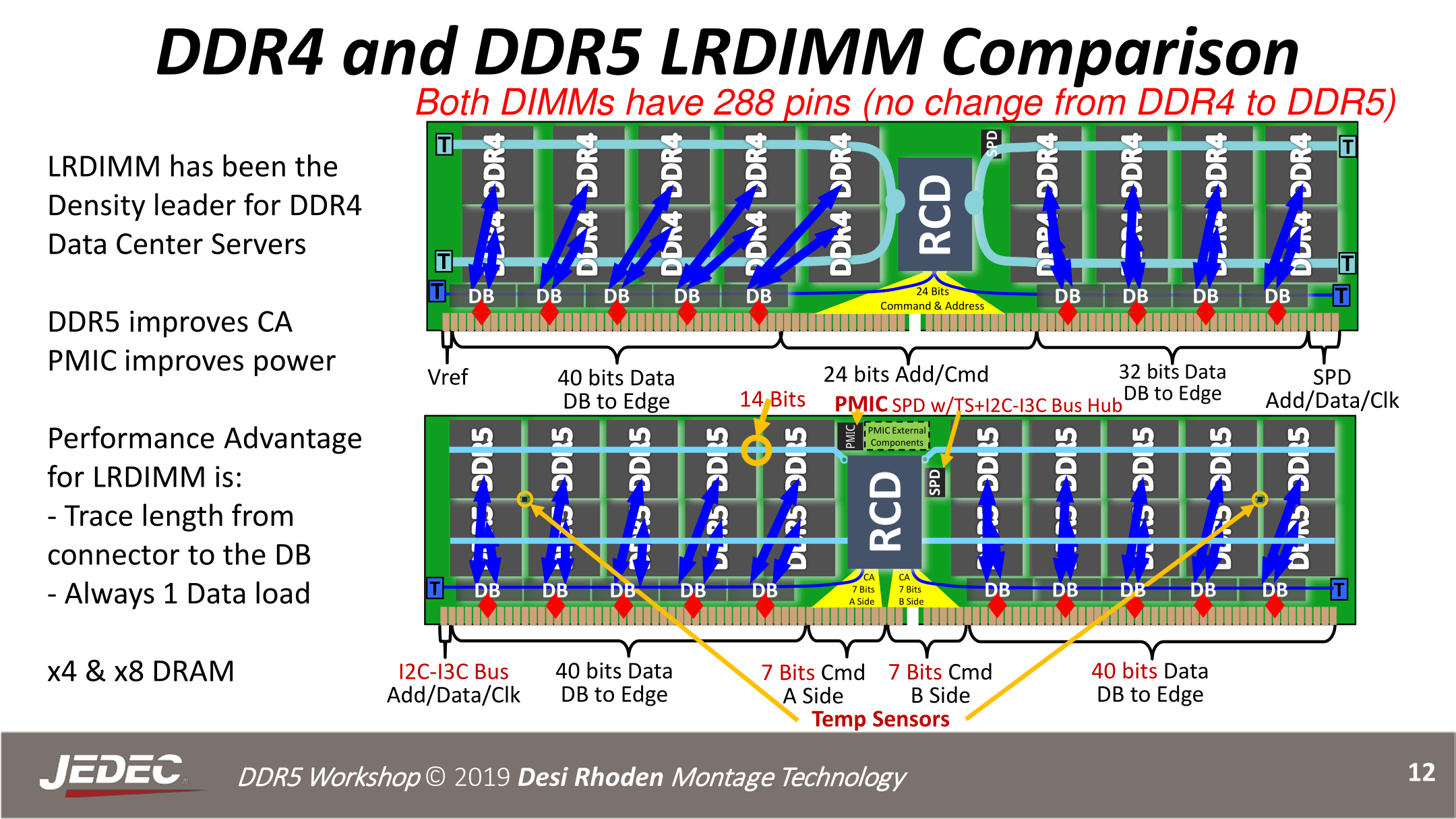
> Consequently, DIMM-wide ECC will still be a thing. Which is why in the JEDEC diagram it shows an LRDIMM with 20 memory packages. That's 10 chips (2 ranks) per channel, with 5 chips per rank. The 5th chip is to provide ECC. Since the channel is narrower, you now need an extra memory chip for every 4 chips rather than every 8 like DDR4.
« The big change here is that the command and address bus is being shrunk and partitioned, with the pins being reallocated to the data bus for the second memory channel. Instead of a single 24-bit CA bus, DDR5 will have two 7-bit CA busses, one for each channel »
If there are two 32-bit data busses rather than one 64-bit bus, arithmetic suggests they shouldn't need to find extra pins from somewhere.
So maybe the rationale for shrinking the CA busses (to 7 rather than 12) is something different?
DDRwhatever is primarily an definition of package level interconnect which has possibility of being used as module level interconnect as one of design constraints. And row hammer and similar things are completely irrelevant for such specifications.
does current hardware and software already allow keeping counts of detected and corrected ECC errors? is it possible for the OS to attribute it to a specific process?
if so it seems like OS'es could track and publically tell on executables
With any sort of decent encryption, flipping a bit will corrupt the entire cache line unpredictably. That's still bad, of course, but it's much less likely to be exploitable.
Doesn't really much help if all the attack is needs to do is flip a flag or replace a value with one that evaluates to true (e.g. anything except 0).
Sure, any particular exploit may be less likely to work, but once you can hammer memory 3/4 of the code running on the system turns into a potential exploit vector. :)
The problem is collateral damage. It's rare that writing garbage to an entire 64-byte (not bit!) cache line will go unnoticed -- in most applications, chances are good that there'll be at least one pointer in there that'll be corrupted.
This is sort of explained in the article. I think they had to use burst length 16 [1] to scale to 6400 MHz, but 16 * 64 bits would be 128 bytes or two cache lines. The whole memory system works in cache lines, so it wouldn't be good if the processor requested one cache line and got two. So they use BL16 with a narrower 32-bit channel to fetch one 64-byte cache line.
As long as multiple cores are accessing memory or prefetching is on (it's almost always on), both channels will be utilized so software won't notice.
[1] When you do a read operation on DRAM you get a multi-cycle burst of data, not just one word. This amortizes command/address overhead and presumably matches the slow-but-wide internal DRAM array with the fast-but-narrow channel. See https://people.freebsd.org/~lstewart/articles/cpumemory.pdf sec. 2.2.
> How is just splitting the memory in two separate channels going to make anything faster?
I am not a HW engineer, but:
With DDR, the difference of all traces in the same channel (data & clock) has very tight tolerances (on the order of 1/8 or 1/16 of a clock). Having fewer traces per channel may make it easier to route for higher clock speeds.
> How will this affect driver complexity and cache-misses?
I'm not sure what you mean? The memory controller should abstract almost all of the differences away. There are per-channel configuration settings that are usually configured by the SPD rom, so there will be twice as many to set, but multichannel memory controllers are already a thing, and going from N to 2N of something doesn't really affect software complexity once N is greater than one.
you can issue two commands simultaneously. yes, the data transfer latency takes twice as long in theory, due to the bus size halving, but with increased clock speeds its not really an issue.
Similarly to how dual channel memory is faster than single channel. Now you can do dual channel with a single stick, or maybe even quad channel with 2 sticks. I believe it should be otherwise transparent to the rest of the system.
I think that's wrong. Going from 1 64-bit channel to 2 32-bit channels has the same throughput per clock (or even slightly lower if the per-transaction overhead is paid separately on each channel).
Yes it can! But, unless I'm mistaken, only within the same bank. This means you can basically only do this for sequential access, not random access.
And there's still a non-zero latency between the responses, so it's still slightly slower than doubling the channels.
Which doesn't answer the question of "why didn't they just double the clock without reducing the bus width" but your answer to the original question sums that up nicely.
Well, you could just increase the clock, but it doesn't really gain you anything. G.Skill already has the F4-4800C18D-16GTRS which runs at 4800Mhz. Is it fast? Not really. The F4-3800C14D-16GTZN running at 3800Mhz is actually faster in practice because you're limited by the memory module's latency.
Increasing the clock just makes it a lot harder for motherboard and CPU manufacturers to support those speeds, but on its own it doesn't really gain you a lot of speed.
Wonder if this spec will make it easy for embedded systems to catch up. It always seems like they lag behind what's cutting edge. Maybe that's a cost/benefit analysis.
I have a brand new design with DDR2. I can power memory from existing 1.8V rail, no need for more voltage regulators. And 400 MHz is totally ok for me since I can have whole memory bandwidth for myself, no operating system, etc. And my application is very cutting edge for sure in its domain.
Despite sounding related, QDR and DDR are mostly unrelated technologies. They are also both poorly named.
The real purpose of DDR is not actually to double the data rate, but to halve your clock speed and allow you to use the same frequency for your clock as your data. This mostly benefits signal integrity.
QDR is better understood as memory with two ports, one for reading and one for writing, which can be used at the same time. This is a lot more expensive and really doesn't have huge benefits for PCs compared to just adding more channels (as DDR5 does).
This may be a stupid point, but, for personal use of computers in their current form, how much memory do you really need? I’m still a little baffled why chrome requires GBs of memory...? Can we have lean software please?
CPUs have become so fast that relative to their "internal" speeds, RAM is the new hard disk. Databases are becoming in-memory, and going out to fixed storage, even SSD, is an anathema.
New applications are not designed to work on data sets bigger than physical memory. Disk-to-disk streaming algorithms are practically unheard of outside of a few niche scenarios. Like I said, even database vendors are moving to in-memory!
I love machines with huge amounts of memory. My laptop has 64 GB, and it's great! I can run entire fleets of servers in a local hypervisor. I can load huge blobs of CSV or JSON data into the shell and not have to worry about the 2-5x overhead of the in-memory representation. It'll fit just fine. I can run every "bloated" app at once and still have 50 GB free for "whatever". I've reindexed a database on my laptop in minutes that would have taken days(!) on a production server because it didn't have enough RAM and was thrashing the storage like crazy.
Another way to look at it is the "GB per CPU core". With existing AMD EPYC 2 CPUs having 64 cores and 128 threads, the typical 512 GB memory configuration is "only" 8 GB per core, or 4 GB per thread! With a dual-socket server, halve those numbers again. Similarly, mainstream desktop Ryzen CPUs have up to 16 cores, and that's not even talking about the not-so-mainstream Threadripper line. For 4GB per core, you'd need 64 GB.
It's likely that AMD will release 24 or 32 core mainstream CPUs in the near future, maybe as soon as 2 years from now when their 5nm products start shipping. I fully expect server CPUs to hit 96-128 cores per socket around the same time frame, or up to 512 hardware threads in a standard two-socket server. Terabytes of memory is going to become "standard" very soon now.
It really is nice when you can afford to have the latest doubling of memory, and do things you couldn't do easily before. Maybe run an entire DC on your computer. Works very well while you're on the upper end.
However, that does not address the sheer wastefulness of our technological trends to require more resources to do things slower, but displayed with smaller and more colorful pixels. Should everyone have a 64-core 512GB memory computer to view web pages, play minecraft or whatever? Will that be too small to write a text document in 20 years time? Will every person on the planet be expected to get a bigger computer because they can't run the (electron-in-ethereum-on-browser-in-container)^n pancomputer?
Wow, someone must be running really lean software if they can run all bloated apps at once and only use 14GB. I switched to 32GB because a single application decided it absolutely needed 8GB RAM.
People always mention more memory usage as a bad thing, but with Moore's Law slowing down, we are being forced to find other ways to speed up computation. One of those ways is trading memory usage for performance via look up tables, caching, duplication, less compact data storage, etc. I would expect memory usage to rise significantly as long as memory technology advances quickly while clockspeeds remain flat.
Based on what's on my existing system I think I could benefit from ~1TB of memory. Above that I'd have to probably try. After maybe ~200GB I bet I'd start to see seriously diminishing returns.
My servers could probably benefit from, idk, petabytes? If I could keep the entirety of my server's hard drive in RAM I'd be very happy.
DRAM runs on a separate process which is dominated by the difficulty of building the capacitors. These are roughly the shape of a pencil (long narrow hexagons) where the central structure which holds the capacitor needs to be etched to perfection in a process that can take days. The transistors underneath are, at that scale, about as large as the chad from a paper hole punch. The capacitors are just about as narrow as material science (limit to voltage arcing through the insulation layers) can make them so there is glacially slow progress in shrinking DRAM further. Meanwhile the transistors are at extreme limits of resolution for liquid immersion processing, as also are the lines needed to join the rows and columns. Getting those perfect requires very specialized and competent processing.
They are not easy, second rate circuits. They are a completely separate branch of the silicon world. Unfortunately since they don't scale much any more, current design methods were mature 8 years ago, the only way you get more of them is to build new factories. That means it is a seller's market in a game where building another fab costs $10B and will only succeed if staffed by really expert people. So, it is generally profitable. The 3 vendors cannot easily undercut each other since they all have roughly the same limits, and any attempt to flood the market takes 4 years to build and everyone can see it coming.
So there you are. DRAM is the pivotal technology of the current computer era. Fixing that will most likely require breakthroughs in fundamental memory technology - or a reason for demand to collapse.