Haha! Infinitely far away (not on my horizon). Thought has crossed my mind, but there are so many other things I want to do first (e.g. audio, superscalar CPU, ...).
They were also really simple to implement in hardware (basically just a small counter that iterates over vector elements while stalling the CPU frontend).
I have not yet scaled up the parallelism internally (by adding more execution units), but I still see performance benefits (less loop logic & branch overhead, less scalar register pressure, less I$ pressure).
And how do the vectors work with branch prediction? If the CPU speculatively starts executing a vector instruction and it turns out it shouldn't, there should be a mechanism to abort the vector sequencing (or nullify the writebacks while letting the vector sequencing play out).
I don't see that in the overview here, but I guess it's just a low-level detail that isn't drawn:
I have dodged most problems with speculation by executing the branch early, before the next instruction can enter the execute stage.
That's one of the reasons why I have very simple branch conditions. E.g. I don't have the MIPS / RISC-V "branch if two registers are equal/not equal/...", only "branch if register is zero/negative/positive/..." - which saves gate delay (if ever so slightly), and makes it possible to invalidate all the following instructions in the pipeline without needing a branch delay slot or advanced speculation logic for instructions that have already entered the EX stages.
In the diagram, as much work as possible is done in "Branch 1" (before register content is available), e.g. calculate the branch target address. All that is done in "Branch 2" is to compare the register value to fixed values (zero and -1) and check the most significant bit (sign bit), and based on the branch condition (from the opcode) determine if the branch was taken or not.
(There is some extra trickery going on in order to handle branch prediction - mostly in parallel to evaluating the branch condition)
Thus, the branch misprediction penalty is three clock cycles.
But why not just do branch delay? Or some sort of prepared branches like on ELBRUS where you can write to predicate register many instrucions ago and take conditional branch at same cost of non-conditional or maybe even prefetch intstructions into second copy of front-end like E2K does. Or some sort of explicit branch slots.
Anyway, I registered here just to reply to you. I kinda want to talk to you more because you do what is interesting for me too.
EDIT: I see you already store "predicates" in registers.
My understanding: Delay slots only make sense when you don't have a branch predictor.
I get the impression that many people massively underestimate how powerful branch prediction is. Even a simple 2 bit saturating counter will correctly predict about 90% of branches, and the accuracy only goes up with better designs.
So why optimise for the uncommon case of incorrectly predicted branches? In the worst case with static branch delay slots, it actually harms branch prediction, because instead of executing the correctly predicted instructions, it's executing the delay slot, which is often a nop because the compiler couldn't find something to put there.
With your other ideas (multiple decoders, explicit delay slots) it's just a question about if it's a good use of resources (design time, transistors, compiler support) to support this uncommon case, or if you might be better off optimising something else like the branch predictor so more code goes down the common path, or just improving the pipeline's throughput in general.
> Delay slots only make sense when you don't have a branch predictor.
Agreed.
I'll go even further: lots of other RISC ideas only really matter when you don't have a branch predictor (and your transistor and design budgets are tiny).
Single-length instructions, for example. Even x86 instructions aren't much of a problem when you can afford to throw more pipeline stages at the problem -- which you can with a branch predictor.
I don't think anybody in the mid-80's understood how good branch predictors can be. Most people probably still didn't really understand it in the early 90's.
> Single-length instructions, for example. Even x86 instructions aren't much of a problem when you can afford to throw more pipeline stages at the problem
I think that the problem is bigger than that. Sure, the branch predictor usually keeps even the x86 pipeline busy, but x86 variable length instruction encoding becomes a problem for at least three problems:
1. Decoding width - There is a practical limit to how many instructions you can decode in parallell. You can add pipeline steps, but at some point it becomes absurd.
2. You get a very big range of minimum-to-maximum number of bytes that you need to fetch to extract a fixed number of instructions each clock. E.g. an eight-wide front-end would have to fetch 8-120 bytes per clock cycle. And it gets worse since your next eight instructions may not start on a nice power-of-two boundary, so you have to fetch much more, e.g. 256 bytes per cycle, in order to cover the worst case scenario (compared 32 bytes per cycle for a fixed width 32-bit RISC encoding). And you may gate cache line / page crossings in your "bundle".
3. Since you need to do fairly heavy translation work into an internal RISC-like encoding (which, by the way can not be as compact as compiler-generated RISC instructions - you typically need 64 bits per internal instruction or similar), you need to cache your translations into a uOP cache (or L0 cache). This cache uses much more silicon per effective instruction than a regular L1I cache, so it can not hold as many instructions (and I'm pretty sure that most of the instructions in the L0 cache are stored in the L1 cache too - so not really extra cache memory). All this silicon could be used for a larger L1I cache, for instance (or a better branch predictor).
So, yes, branch prediction really helps, but it does not solve all problems.
> 1. Decoding width - There is a practical limit to how many instructions you can decode in parallell. You can add pipeline steps, but at some point it becomes absurd.
Branches. Branches also make really wide decodes useless. The cost/benefit is towards wider decoders for A64 than for AMD64. The average A64 instruction does slightly less work than the average AMD64 instruction so the net result is that it makes sense to have slightly wider decoders (in terms of "work") for A64 than for AMD64.
X86 CPUs don't quite use a "RISC-like encoding". The µops support RMW for memory, for example. The encoding is of course very much regularized, but I don't think the RISC people have a patent on that.
Translation to an internal format is common for high-performance RISC CPUs as well. The Power CPUs call it "cracking" when complicated instructions are split into simpler µops.
> The average A64 instruction does slightly less work than the average AMD64 instruction so the net result is that it makes sense to have slightly wider decoders
I'm not sure that the difference is that big. A64 actually has quite powerful instructions, and some of them do more work than similar x86 instructions (madd and ubfx come to mind). In my testing A64 code often has fewer instructions than x86: https://www.bitsnbites.eu/cisc-vs-risc-code-density/
> X86 CPUs don't quite use a "RISC-like encoding". The µops support RMW for memory, for example.
I would love to learn more about that. Do you have any references? I was under the impression that internal instructions followed the load/store principle since I assume that the internal pipeline is a load/store pipeline?
> The Power CPUs call it "cracking" when complicated instructions are split into simpler µops.
Yes, it's the IBM term AFAIK. They call it cracking in zArch too. I also suapect that at least some ARMv8/9 implementations do cracking too (many AArch64 instructions have multiple results, which might be better handled as multiple internal instructions - I think it's partly a code density thing).
> I was under the impression that internal instructions followed the load/store principle since I assume that the internal pipeline is a load/store pipeline?
Well... peterfirefly is making a very generalised statement that isn't really true.
As far as I'm aware, no out-of-order Intel processor can do a full read-modify-write in a single uOP. And if you go all the way back to the original P6 pipeline (Pentium Pro, Pentium II, Pentium III), it does appear to be a proper load-store arch. RMW instructions generate at least 4 uOPs
But the Pentium M and later can do a read + modify to register in a single fused uOP, and a RMW in just two fused uOPs. Fused uops kind of muddle the issue: they might issue to two or more execution units, but for the purposes of scheduling, they only take up a single slot.
So it's far from a proper load/store pipeline. And when you think about it, that makes sense, x86 isn't a load/store ISA so it would be wasteful to not have special accommodations for it.
-----
And then there is AMD. Zen and later are more or less identical to Intel's modern fused uOP scheme.
But their older cores had much more capable internal encoding which AMD called "macro-ops". And those macro-ops could do a full read-modify-write operation with a single op. Unlike Intel and the later Zen core, each integer execution unit needed to have both ALUs and AGUs, along with read/write ports to the data cache.
> I would love to learn more about that. Do you have any references?
Agner Fog is the best resource for this type of thing.
A combination of microarchitecture.pdf for details about the various pipelines and instruction_tables.pdf for what uops the various instructions breakdown into on the various pipelines.
Thanks, I have read the Agner documents before. I will dig around some more and get updated.
Anyway, I found this, regarding RMW (for Ice/Tiger Lake):
> Most instructions with a memory operand are split into multiple μops at the allocation stage. Read-modify instructions, such as add eax,[rbx], are split into two μops, one for address calculation and memory read, and one for the addition. Read-modify-write instructions, such as add [rbx],eax, are split into four μops.
I read it as a instructions that use memory operands (other than simple mov instructions) are usually split into at least two uOPs, which makes perfect sense for a load/store pipeline.
> So it's far from a proper load/store pipeline. And when you think about it, that makes sense, x86 isn't a load/store ISA so it would be wasteful to not have special accommodations for it.
The way I see it, modern x86 microarchitectures are load/store. My definition of load/store is that all instructions/operations that flow through the execution part of the pipeline can either load/store data OR perform operations on registers, not both (except possibly edge cases like calculating an address or writing back an updated address to a register).
That is by far the most efficient way to implement a CPU pipeline: You don't want to read data in one pipeline stage, use the data in an ALU in a later stage, and possibly write data in an even later stage. That would drastically increase instruction latency and/or require duplication of resources.
This is, AFAIK, one of the main advantages and probably the raison d'être for uOPs is the first place: translate x86 instructions into uOPs (multiple ones for instructions that access memory) so that the pipeline can be implemented as a traditional load/store pipeline.
In a way the x86 front end is similar to software binary translation (a'la Transmeta, NVIDIA Denver or Apple Rosetta 2). It's fairly complex, and the prime objective is to take code for a legacy ISA and transform it into something that can run in a pipeline that the ISA was originally not intended to run in. By doing the translation in hardware you avoid the latencies inherent to software translation (JIT or AOT), but the costs are unavoidable (particularly silicon area and power consumption).
It's only a load/store architecture if you consider the "unfused-uop" to be the native internal ISA of the underlying pipeline.
But that seems to be an incorrect perspective. The pipeline's native internal ISA appears to very much be the "fused-uop". It's the only metric which matters for most of the pipeline, decode limits are specified in fused-uops, the uop cache stores fused uops, the ROB only uses a single entry for fused-uop.
The only part of the pipeline were that deals with unfused-uops is the scheduler and the execution units themselves. Even the retire stage works on fused-uops.
It's probably better to think of the pipeline's native ISA as an instruction that can sometimes be scheduled to two execution units. It's almost a very basic VLIW arch, if you ignore the dynamic scheduling.
Sure, the execution units are load/store. And the scheduling is load/store. But I don't think that's enough to label the entire pipeline as load/store since absolutely every other part of the pipeline uses fused-uops and is therefore not load/store.
> This is, AFAIK, one of the main advantages and probably the raison d'être for uOPs is the first place: translate x86 instructions into uOPs so that the pipeline can be implemented as a traditional load/store pipeline.
I'm really not a fan of the "translate" terminology being used to describe modern x86 pipelines. It's not quite wrong, but it does seem to mislead people (especially RISC fans) into overstating the nature of the transformation.
It's nothing like software binary translation (especially something like Rosetta 2), the transforms are far simpler. It's not like Intel took an off-the-shelf RISC architecture and limited their efforts to just designing a translation frontend for it (the few examples of direct hardware translation, like NVIDIA Denver and Itanium have pretty horrible performance in that mode).
No, they designed and evolved the pipeline and its internal ISA to directly match the x86 ISA they needed to run.
All the front end is really doing is regularising the encoding to something sane and splitting up some of the more complex legacy instructions. Instructions with memory operands are converted to a single fused-uop. The front-end only splits the read-modify-write instructions into two fused-uops.
The transform into proper load/store form doesn't happen until much further down the pipeline as the fused-uop gets inserted into the scheduler.
I have quite a bit of experience writing software binary translation software, and I ensure you such translations are significantly more complex than the transforms you find inside an x86 pipeline.
> Thanks, I have read the Agner documents before. I will dig around some more and get updated.
I swear every single time I read them (or usually just parts of them) I learn more about x86 microarches (and CPU design in general). It's not something that can be absorbed in a single pass.
Good points. I guess it's a debate of nomenclature, which lacks real importance (although it helps to reduce confusion).
My point of view is mostly that, no, the x86 architecture certainly is not load-store, but internally modern x86 machines have execution pipelines that are built like regular load-store pipelines (i.e. the topology and flow is mostly the same as a RISC-style load-store pipeline).
Or to put it another way, x86 execution pipelines are much closer to being register-register than being register-memory.
> No, they designed and evolved the pipeline and its internal ISA to directly match the x86 ISA they needed to run.
Yes. That is very true. Although the front end is the part of the pipeline that is most x86-specific, there are many parts of the rest of the pipeline that is tailored to be optimal for x86 code. It was obviously not designed in a vacuum.
An interesting observation is that even other ISA:s and microarchitectures have been influenced by x86 (e.g. by including similar flags registers in the architectural state), in order to not suck at emulation of x86 code.
> I guess it's a debate of nomenclature, which lacks real importance (although it helps to reduce confusion).
Agreed. I wouldn't be pedantic about this for a higher level discussion, but when you start to get into the weeds of what a modern x86 pipeline is, it's starts to matter.
> (i.e. the topology and flow is mostly the same as a RISC-style load-store pipeline).
So that brings up an interesting question. What is a RISC-style pipeline?
Everyone mostly agrees what a RISC-style ISA is, usually focusing on the load/store arch and fixed length instructions (and exposed pipeline implementation details was another common attribute of early RISC ISAs, but everyone now agrees that was a bad idea).
But nobody ever seems to define "RISC-style pipeline", or they allude to overly broad definitions like "Everything that's not CISC" or "any pipeline for a RISC-style ISA". But you might have noticed that I like more precision in my nomenclature. And modern x86 CPUs prove the point that just because something is executing a CISC like ISA doesn't mean the pipeline is also CISC. There is nothing stopping someone implementing a CISC style uarch for a RISC style ISA (other than the fact it's a stupid idea).
I like to make a the bold argument the definition of "RISC-style pipeline" should be limited to simple in-order pipelines that are optimised for high-throughput that approaches one instruction per cycle (or group of instructions for super-scalar designs). The 5-stage MIPS pipeline is probably the most classic example of a RISC pipeline and the one usually taught in cpu architecture courses. But it ranges from 3 stage pipeline of Berkley RISC and early ARM chips to... well I think we have to include the PowerPC core from the PowerPC and Xbox 360 in this definition, and that has something like 50 stages.
(BTW, I also like to exclude VLIW arches from this definition of a RISC-style pipeline, sorry to everyone like Itanium and Transmeta)
Your 8 stage MRISC32 pipeline is a great sample of a modern RISC-style pipeline and along with all the in-order cores from ARM that are often around the same length.
But this does mean I'm arguing that anything with out-of-order execution is not RISC. Maybe you could argue that some simpler out-of-order schemes (like the early powerpc cores) aren't that far from RISC pipelines because they only have very small OoO windows. But by the time you get to the modern high-preformance paradigm of many instruction decoders (or uop caches) and absolutely massive re-order buffers, unified physical register file and many specialised execution units.
It's very much a different architecture to the original RISC-style pipelines, even if they still implement a RISC style ISA. It's an architecture that we don't have a name for, but I think we should. Intel pioneered this architecture starting with the P6 pipeline and perfecting it around the time of Sandybridge, and then everyone else seems to copying it for their high-performance cores.
I'm going to call this arch the "massively out-of-order" for now.
------------
Anyway, I wanted to switch to this way more precise and pedantic definition of "RISC-style pipeline" so that I could point out a key difference in the motivation in why Intel adopted this load-store aspect to their pipeline compared to RISC-style pipeline.
RISC-style pipelines are load-store partly because it results in a much more compact instruction encoding and allows fixed-length instruction, but mostly because it allows for a much simpler and more compact pipeline. The memory stage of the pipeline is typically after the execute stage. If a RISC-style pipeline needed to implement register-memory operations, they would need to move the execute stage after the memory stage completes, resulting in a significantly longer pipeline. And very problematic for the most pure RISC-style pipelines that don't have branch predictors and are relying on short their pipelines and branch-delay slots for branch performance.
A massively out-of-order x86 pipeline gets neither advantage. The instruction encoding is still register-memory (plus those insane read-modify-write instructions), and the cracking the instructions into multiple uops causes extra pipeline complexity. Also, they have good branch predictors.
The primary motivation for cracking those instructions is actually memory latency. Those pipelines want to be able to execute the memory uop as soon as possible so that if they miss in the L1 cache, the latency can be hidden.
This memory latency hiding advantage is also one of the major reasons why modern high-performance RISC cores moved away from the RISC-style pipeline to adopt the same massively out-of-order pipelines as x86. They just have a large advantage in the fact that their ISA is already load/store.
I see what your pointing at. I don't think that we'll fully agree on the nomenclature, but this kind of feels like the RISC vs CISC debate all over again. The reality is that the waters are muddied from the 1990's and onward.
I know that I have a tendency to over-use the word "RISC" (basically for anything that is not a 70's CISC state-machine).
> or they allude to overly broad definitions like "Everything that's not CISC"
Yup, that's me ;-)
BTW, w.r.t. nomenclature, I make a clear distinction between "architecture" and "microarchitecture" (even if I mix up contexts at times).
> But this does mean I'm arguing that anything with out-of-order execution is not RISC.
I think that this is where we disagree. E.g. the POWER1 (1990) was the first (non-mainframe) out-of-order CPU with register renaming, and it was a RISC. The Alpha 21264 (1998) was definitely both RISC and OoO. One of the first x86 implementations with uOPs translation, the NexGen Nx686 (1995, later AMD K6), was also out-of-order, and was said to have a RISC microarchitecture (based on RISC86). Not as complex as modern cores, but drawing the line at OoO does not work for me.
Historically RISC meant many things, and as you said the early RISC machines had many design quirks that did not stand the test of time (in particular exposing too many microarchitectural details in the ISA - something that proved useful in low-power VLIW DSP:s, though).
However, the key takeaway that has stood the test of time is an instruction set that enables fully pipelined execution. In the 70's and 80's, using a load-store (register-register) ISA was the only viable way out of multi-cycle instructions. To me, the principle to design instructions for pipelined execution is the main point of RISC, and the key point where it differs from CISC ISA:s, which were specifically designed for state-machine style microarchitectures (I don't have a better term).
In the 90's the same principles were implemented at the microarchitecture level (Nx586, K6, P6), without changing the architecture (i.e. the x86 ISA was kept on the surface).
Out-of-order happened to arrive to microprocessors at around the same time, so it was an obvious natural development for all high-performance CPU:s, regardless of "RISC" branding or not. It was the way forward to increase ILP (yes, you can do superscalar in-order too, but there's a rather annoying limit to parallelism there). It just so happened that cracking x86 instructions into multiple uOPs was a good way to make better use of OoO as well (in fact, that kind of cracking was exactly what was proposed by the RISC crowd in the 70's and 80's, but at the ISA level rather than at the microarchitecture level).
> I'm going to call this arch the "massively out-of-order" for now.
Mitch Alsup calls it GBOoO (Great Big Out-of-Order). There are some merits to making that distinction - but like you I would like to see a widely adopted definition.
Yet, I will continue to use terms like "RISC-like pipeline". I guess one of my main motivations is to make people understand that x86 is no longer CISC "under the hood". Especially with RISC-V being popularized, a new generation comes asking questions about RISC vs CISC (as in RISC-V vs x86), without understanding the difference between an architecture and a microarchitecture.
For most intents and purposes most GBOoO microarchitectures are comparable when it comes to the execution pipeline, regardless of which ISA they are using. The main differences are in the front end - but even there many of the principles are the same (it's mostly a question of how much effort needs to be spent on different parts - like decoding, prediction, caching).
Correction: Ok, the IBM z/Architecture line of CPU:s are clearly a different breed. In later generations they do use instruction cracking (i think that they were inspired by the x86 success), and insane pipelines:
> Mitch Alsup calls it GBOoO (Great Big Out-of-Order).
I like that term. Do you have any suggested reading material from Alsup?
------------
> I see what you're pointing at. I don't think that we'll fully agree on the nomenclature,
Ok, I admit I might be going a little far by trying to redefine anything that isn't a classic in-order RISC pipeline as "not RISC" (even when they have a RISC style ISA). And as an amateur CPU architecture historian, I'm massively underqualified to be trying to redefine things.
I'm also not a fan of the fact that my argument defines any pipeline with any amount of OoO as "not RISC". Because I do know the early PowerPC pipeline quite well (especially the 750 pipeline), and the amount of out-of-order is very limited.
There is no reorder buffer. There is no schedule, instead dispatch only considers the next two instructions in the instruction queue, and there is only one reservation station per execution pipeline. For the 601, there are only three pipelines (Integer, FPU and Special) and branches are handled before dispatch. So while a branch or FPU instruction might be executed before an Integer instruction, you can't have two instructions for the same pipeline execute out of order.
I don't think the 601 even has renaming registers, there is no need as Integer instructions, Floating instructions AND branch instructions all operate on different register sets (and I'm just realising exactly why PowerPC has those seperate condition registers)
Now that I think about it, the 601 pipeline might be described as a superscalar in-order RISC pipeline that simply relaxes the restriction on the different execution pipes starting out of program order.
Maybe I should be altering my argument so to allow simpler out-of-order schemes to still be considered RISC. The 601 is certainly not something us people from the future would recognise as OoO except by the strictest definition of somethings instructions execute out-of-order.
The later PowerPC designed do muddy the water; The 604 (1996) introduces the concept of multiple integer pipelines that can execute the same instructions. They only have one reservation station each, but this will allow instructions of the same type to be executed out of order via different pipeline. The load/store instructions were moved to their own pipeline, in the later 750 design (aka the G3, 1997), the load store pipeline gained two reservation stations, allowing memory instructions to be executed out of order down the same pipeline.
It's not until the PowerPC 7450 (aka the G5, 2001) that the PowerPC finally gained something approaching a proper scheduler, removing the one reservation station per pipeline bottleneck.
> E.g. the POWER1 (1990) was the first (non-mainframe) out-of-order CPU with register renaming, and it was a RISC.
As I understand, the POWER1 is about the same as the PowerPC 601. There is no register renaming, the only out-of-order execution is the fact that branch instructions execute early, and floating point instructions can execute out of order with respect to integer instructions.
I don't think there is a RISC cpu with register renaming until the PowerPC 604 in 1996 or maybe PowerPC 750 in 1997, and that was very limited, only a few renaming registers.
---------------
> but this kind of feels like the RISC vs CISC debate all over again
Yes. And my viewpoint originates from my preferred answer to the RISC vs CISC debate. That they are outdated terms that belong to the high-performance designs of 80s and early 90s, and don't have any relevance to modern GBOoO designs (though RISC does continue to be relevant for lower-power and low area designs)
> I guess one of my main motivations is to make people understand that x86 is no longer CISC "under the hood"
We both agree that GBOoO designs aren't CISC. I'm just taking it a step further in saying they aren't RISC either.
But my preferred stance leads to so many questions. If such designs aren't RISC then what are they? Where should the line between RISC and not-RISC be drawn? If we are allowing more than just two categories, then how many more do we need?
It's certainly tempting to adopt your "everything is either CISC or RISC" stance just to avoid those complicated questions, but instead I try to describe lines.
And I think you agree with me that having accepted definitions for groupings of related microarchitectures would be useful, even if you want them to be sub-categories under RISC.
> BTW, w.r.t. nomenclature, I make a clear distinction between "architecture" and "microarchitecture" (even if I mix up contexts at times).
Yeah, I try to avoid "architecture" all together, though I often slip up. I use ISA for the instruction set and microarchitecture or uarch for the hardware implementation.
----
> However, the key takeaway that has stood the test of time is an instruction set that enables fully pipelined execution...
So I agree with all this. I think what I'm trying to do (this conversation is very helpful for thinking though things) is add an additional restriction that RISC is also about trying to optimise that pipeline to be as short as possible.
Pipeline length is very much the enemy for in-order pipelines. The longer the back-end have, the more likely you are to have data hazards. And a data hazard is really just a multi-cycle instruction in disguise. This is a major part of the reason why RISC always pairs with load/store.
Also the more stages you have in the front-end, the larger your branch misprediction delay (and in-order pipelines are often paired with weak branch predictors, if they have one at all).
But the switch to the GBOoO style architecture has a massive impact on this paradigm. Suddenly, pipeline length stops being so critical. You still don't want to go crazy, but now your scheduler finds different instructions to re-order into the gaps that would have been data hazard stalls in an in-order design. And part of the price you pay for GBOoO is a more complex frontend (even a RISC ISA requires extra complexity for OoO over In-order), but you are happy to pay that cost because of the benefits, and the complex branch predictors help mitigate the downsides.
(I don't know where Alsup wants to draw the line for GBOoO, but I'm taking OoO designs with proper schedulers and ROBs with dozens of entires. Designs like the early PowerPC chips with their limited OoO don't count, they were still very much optimising for short pipeline lengths)
I'm arguing that this large paradigm shift in design is enough justification to draw a line and limit RISC to just the classic RISC style pipelines.
> the NexGen Nx686 (1995, later AMD K6), was also out-of-order, and was said to have a RISC microarchitecture (based on RISC86).
I don't like relying on how engineers described or how the marketing team branded their CPU design for deciding if a given microarchitecture is RISC or not. RISC was more of a buzzword than anything else, and the definition was muddy.
A major point against the NexGen line being RISC (including all AMD designs from the K6 to Bulldozer etc) is that they don't crack register-memory instructions into independent uops. I pointed this previously, but their integer pipelines can do a full read/modify/write operation with a single uop. I don't know about you, but I'm pretty attached to the idea that RISC must be load/store.
This is also part of the reason why I want more terms than just RISC and CISC. Because the NexGen line is clearly not CISC either.
And we also have to consider the other x86 designs from the 486 and 586 era. They are fully pipelined and even superscalar, but they don't crack up register-memory ops, and their pipelines haven't been optimised for length, so it would be wrong to label them as RISC or RISC-like.
But they are so far from the "state-machine style microarchitectures" (and I think that's a perfectly fine term) that CISC originated from that I think it's very disingenuous to label them as CISC or CISC-like either.
> For most intents and purposes most GBOoO microarchitectures are comparable when it comes to the execution pipeline, regardless of which ISA they are using. The main differences are in the front end - but even there many of the principles are the same
The execution pipelines themselves might be very comparable, but you are forgetting the scheduling, which adds massively to backend complexity, and makes a major impact to the overall microarchitecture and the design paradigms.
> As I understand, the POWER1 is about the same as the PowerPC 601. There is no register renaming
Yes, it's a stretch to call it an OoO implementation with register renaming. I think that it does register renaming, but only for the FPU, and only in a very conservative way. Merely pointing out that OoO and register renaming weren't really pioneered in x86 architectures in the late 1990's. As usual, it's an incremental process, with no clear start.
> and the definition was muddy
And it still is ;-)
> This is also part of the reason why I want more terms than just RISC and CISC. Because the NexGen line is clearly not CISC either.
Agree. I think that many of the confusions are around ISA and microarchitecture. E.g. do all x86 CPU:s count as CISC, since the ISA is CISC? Does the internal uOP instruction set qualify as an "architecture" (ISA)? How about the decoded "operation packets" that flow down the execution pipeline? Can you even say that a microarchitecture is "RISC", or is that term reserved for the architecture?
I think I lack a good term for "a straight pipeline without loops" (or thereabout), which is kind of the original watershed between CISC and RISC, back when architecture and microarchitecture were still very intimately coupled (remember, CISC too exposed to much of the microarchitectural details, which is one of the main reasons that we have an "x86 tax" in the first place).
z/Architecture is an interesting extreme to bring into the mix, since even though it does pipelining, most of the implementations have a fairly complex "graph" rather than a straight line (AFAICT). It can't be made to resemble RISC even if you squint, whereas it can be hard to tell the pipelines for AArch64, POWER9 and x86-64 implementations apart at a quick glance: They all have a very clear and straight flow.
> this conversation is very helpful for thinking though things
Exactly :-) I love these discussions as I find that when I try to explain or argue a certain topic, many pieces fall into place, plus of course you pick up and learn tons from people like you who know a lot and clearly have given these questions some thought.
> but you are forgetting the scheduling, which adds massively to backend complexity, and makes a major impact to the overall microarchitecture and the design paradigms
I think I'm merely dismissing it as "yet another major technical improvement" (right up there with pipelining, caches, branch prediction, and superscalar execution). It surely is a major microarchitecture paradigm, and it does seem to be one that will stick for a long time, but I'm still reluctant to compare it to CISC or RISC, which in my mind talk more about the architectecture, whereas GBOoO talks more about the microarchitecture, and is largely ISA agnostic (these days). Gaah, it's hard. Going back to the question about ISA vs uarch again.
I think it's a bit strong to say that branch prediction "solves" the problem of x86's complex variable length encoding. But it certainly goes a long way to mitigating the handicap, and allowing x86 uarches to be very competitive with more RISC designs.
I suspect that original handicap is a large part of the reason why x86 managed to become a dominant ISA, beating out all of its RISC derived competitors in the high-performance space. The requirement to continue supporting the legacy complex instruction encoding forced x86 uarch designers to go down the path of longer (but not too long) pipelines, powerful branch predictors and extremely large out-of-order windows.
It wasn't the obvious approach back in the 90s/2000s, high-performance RISC designs of that era tended to stick with in-order superscalar pipelines. And when they did explore out-of-order designs, they were much more restrained with way smaller reorder-buffers.
But in hindsight, it seems to have been the correct approach for high-performance micro arches. I can't help but notice that modern high-performance aarch64 cores from Apple and Arm have pipelines that look almost identical to the designs from AMD and Intel. Main difference is that they can get away with 8-wide instruction decoders instead of a uOP caches.
> which, by the way can not be as compact as compiler-generated RISC instructions - you typically need 64 bits per internal instruction or similar
Nah. According to Agner Fog's testing, Intel only allocates 32bits per uop.
Immediates/Addresses larger than signed 16bits are handled with various complex mechanisms. If a 32bit/64bit value is still inside the -2¹⁵ to +2¹⁵ range, it can be squashed down. Space can be borrowed from other uOPs in the same cacheline that don't need to store an immediate. Otherwise, the uOP takes up multiple slots in the uOP cache.
I suspect AMD also use a similar mechanism, because as you point out, caching un-encoded uOPs would be a huge waste of space. And there is no reason why you need to use the exact same encoding in both the pipeline and the uOP cache, it just needs to be significantly easier to decode than a full x86 instruction.
If they are correct, the uOP cache consumes at least as much silicon as the L1I cache, while they generally can hold fewer instructions.
Some napkin math: x86 instructions are 4 bytes long on average, so a 32KiB L1I can hold 32/4=8K instructions, while the uOP cache can hold 4K uOP instructions (how many uOPs does an x86 instruction translate to on average?). That would indicate that uOP:s require twice the silicon area to store compared to "raw" x86 instructions - or that the uOP cache is more advanced/complex than the L1I cache (which may very well be the case).
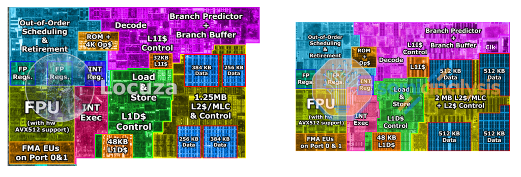
Also visible from the die shots: decoding and branch prediction are far from free.
According to the label, that block contains both the uop cache AND the microcode ROM (which is actually at least partially RAM to allow for microcode updates). I guess it makes sense to group the two functions together, they are both alternative sources of uOPs that aren't from the instruction decoder.
So really depends on what the balance is. If it was two or three of those memory cell blocks, I agree it's quite big. But if it's just one, it's actually quite small.
Agner's findings are for the Sandybridge implementation. He says Haswell and Skylake share the same limitations, but doesn't look like he has done much research into the later implementations.
The findings actually point to the uOP cache being much simpler in structure. The instruction cache has to support arbitrary instruction alignment and fetches that cross boundaries. The uOP cache has strict alignment requirements, it delivers one cache line per cycle and always delivers the entire line. If there aren't enough uops, then the rest of the cacheline is unused.
> Also visible from the die shots: decoding and branch prediction are far from free.
Yeah, it appears to be massive. And I get the impression that block is more branch prediction than decoding.
Nothing is free in CPU design, it's just a massive balancing act.
> According to the label, that block contains both the uop cache AND the microcode ROM
Yes, so it's hard to tell the exact size. We can only conclude that the uOP cache and the microcode ROM combined are about twice the size of the L1I cache (in terms of memory cells).
Here uCode is in a separate area, and if we assume that the SRAM blocks in the area marked "Decode" represent the uOP cache, then we have:
* The uOP cache has the same physical size as the L1I cache
* uOP cache size = 4K uOPs
* L1I cache size = 32 KiB ~= 8K x86 instructions
If all this holds true (it's a big "if"), the number of uOP instructions that the uOP cache can hold is only half of the number of x86 instructions that the L1I cache can hold, and the size of uOP entries are in fact close to 32KiB / 4K uOPs = 64 bits each (given how similar the SRAM cells for the two caches are on the die shot I assume that they have the same density).
Furthermore I assume that one x86 instruction translates to more than one uOP instruction on average (e.g. instructions involving memory operands are cracked, and instructions with large immediates occupy more than one uOP slot - even the ARMv8 Vulcan microarchitecture sees a ~15% increase in instructions when cracking ARM instructions into uOPs: https://en.wikichip.org/wiki/cavium/microarchitectures/vulca... ), which would mean that the silicon area efficiency of the uOP cache compared to a regular L1I cache is even less than 50%.
Edit:
> Nothing is free in CPU design, it's just a massive balancing act.
Yup, and a large part of the x86 balancing act is to keep the x86 ISA alive and profit from the massive x86 ecosystem. Therefore Intel and AMD are prepared to sacrifice certain aspects, like power efficiency (and presumably performance too), and blow lots of energy on the x86 translation front end. That is a balancing act that designers of CPU:s with more modern ISA:s don't even have to consider.
Pretty strong evidence that AMD are using a much simpler encoding scheme with roughly 64bits per uop. Also, That uop cache on Zen 4 is starting to look ridiculously large.
But that does give us a good idea how big the microcode rom is. If we go back to the previous intel die shot with its combined microcode rom + uop cache, it appears intel's uop cache is actually quite small thanks to their better encoding.
> Furthermore I assume that one x86 instruction translates to more than one uOP instruction on average (e.g. instructions involving memory operands are cracked
I suspect it's not massively higher one uop per instruction. Remember, the uop cache is in the fused-uop domain (so before memory cracking) and instruction fusion can actually squash some instructions pairs into a single uop.
The bigger hinderance will be any rules that prevent every uop slot from being filled. Intel appears to have many such rules (at least for Sandybridge/Haswell/Skylake)
> and blow lots of energy on the x86 translation front end
TBH, we have no idea how big the x86 tax is. We can't just assume the difference in performance per watt between the average x86 design and average high performance aarch64 design is entirely caused by the x86 tax.
Intel and AMD simply aren't incentivised to optimise their designs for low power consumption as their cores simply aren't used in mobile phones where ultra low power consumption is absolutely critical.
No, and it gets even more uncertain when you consider different design targets. E.g. a 1000W Threadripper targets a completely different segment than a 10W ARM Cortex.Would an ARM chip designed to run at 1000W beat the Threadripper? Who knows?
> Intel and AMD simply aren't incentivised to optimise their designs for low power consumption as their cores simply aren't used in mobile phones where ultra low power consumption is absolutely critical.
They'll keep doing their thing until they can't compete. They lost mobile and embedded, and competitors are eating into laptops and servers where x86 continues to have a stronghold. But perf/watt matters in all segments these days, and binary compatibility is dropping in importance (e.g. compared to 20-40 years ago), much thanks to open source.
IMO the writing is on the wall, but it will take time (especially for the very slow server market).
Yeah, I agree that the writing is on the wall for x86. As you said, power consumption does matter for laptops and server farms.
I'm a huge fan of aarch64, it's a very well designed ISA. I bought a Mac so I could get my hands of a high-preformance aarch64 core. I love the battery life and I'm not going back.
I only really defend x86 because nobody else does, and then people dog pile on it talking it down and misrepresenting what a modern x86 pipeline is.
Though I wouldn't write x86 off yet. I get the impression that Intel are planning to eventually abandon their P core arch (the one with direct lineage all the way back to the original Pentium Pro). They haven't being doing much innovation on it.
Intel's innovation is actually focused on their E core arch, which started as the Intel Atom and wasn't even out-of-order. It's slowly evolved over the years with a continued emphasis on low-power consumption until it's actually pretty completive with the P core arch.
If you compare Golden Cove and Gracemont, the frontend is radically different. Golden Cove has a stupid 6 wide decoder that can deliver 8 uops per cycle... though it's apparently sitting idle 80% of the time (power gated) thanks to the 4K uop cache.
Gracemont doesn't have a uop cache. Instead it uses the space for a much larger instruction cache and two instruction encoders running in parallel, each 3-wide. It's a much more efficient way to get 6-wide instruction decoding bandwidth, I assume they are tagging decode boundaries in the instruction cache.
Gracemont is also stupidly wide. Golden cove only has 12 execution unit ports, Gracemont has 17. It's a bit narrow in other places (only 5 uops per cycle between the front-end and backend) but give it a few more generations and a slight shift in focus and it could easily outperform the P core. Perhaps add a simple loop-stream buffer and upgrade to three or four of those 3-wide decoders running in parallel.
Such a design would have a significantly lower x86 tax. Low enough to save them in the laptop and server farm market? I have no idea. I'm just not writing them off.
> I'm a huge fan of aarch64, it's a very well designed ISA
I totally agree. I would go as far as to say that it's the best "general purpose" ISA available today. I am under the impression that the design was heavily data driven, building on decades of industry experience in many different sectors and actually providing efficient instructions for the operations that are used the most in real code.
> I only really defend x86 because nobody else does
:-D I can easily identify with that position.
> I get the impression that Intel are planning to eventually abandon their P core arch
Very interesting observation. It makes a lot of sense.
I also think that we will see more hybrid solutions. Looking at the Samsung Exynos 2200, for an example from the low-power segment, it's obvious that the trend is towards heterogeneous core configurations (1 Cortex-X2 + 3 Cortex-A710 + 4 Cortex-A510): https://locuza.substack.com/p/die-analysis-samsung-exynos-22...
Heterogeneous core configurations has only just recently made it to x86, and I think it can extend the lifetime of x86.
For laptops, I can see an x86 solution where you have a bunch of very simple and power-efficient cores in the bottom, that perhaps even uses something like software-aided decoding (which appears to be more power-efficient than pure hardware decoding) and/or loop buffers (to power down the front end most of the time). And then build on top of that with a few "good" E-cores, and only one or two really fast cores for single-threaded apps.
For servers I think that having many good E-cores would be a better fit. Kind of similar to the direction AMD is taking with their Bergamo EPYC parts (though technically Bergamo is not an E-core, it gives more cores at the same TDP).
> I am under the impression that the design was heavily data driven, building on decades of industry experience in many different sectors and actually providing efficient instructions for the operations that are used the most in real code.
Yeah, that's the impression I get too. I also get the impression they were planning ahead for the very wide GBOoO designs (I think Apple had quite a bit of influence on the design and they were already working a very wide GBOoO microarch), so there is a bias towards a very dense fixed-width encoding, at the expense of increased decoding complexity.
ARM weren't even targeting the ultra low end, as they have a completely different -M ISA for that.
This is in contrast to RISC-V. Not only do they target the entire range from ultra low end to high performance, but the resulting ISA feels like it has a biased towards ultra low gate count designs (the way immediates are encoded are points towards this).
---------------
You might hate me for this, but I have to raise the question:
Does AArch64 actually count as a RISC ISA?
It might have the fixed width encoding and load/store arch we typically associate with RISC ISAs. But there is one major difference that arguably disqualifies it on a technicality.
All the historic RISC ISAs were designed in parallel with the first generation microarchitecture of the first CPU and where hyper-optimised for that microarchitecture (often to a fault, leaving limited room for expansion and introducing "mistakes" like branch delay slots). Such ISAs were usually very simple to decode, which lead to the famous problems that RISC had with code density.
I lean towards the opinion that this tight coupling between ISA and RISC microarchitecture is another fundamental aspect of a RISC ISA.
But AAarch64 was apparently designed by committee, independent of any single microarchitecture. And they apparently had a strong focus on code density.
The result is something that is notably different from any other RISC ISA.
You could make a similar argument about RISC-V, it was also designed by committee, independent of any single microarchitecture. But they also did so with an explicit intention make a RISC ISA, and the end result feels very RISC to me.
> that perhaps even uses something like software-aided decoding (which appears to be more power-efficient than pure hardware decoding)
At this point, I have very little hope for software-aided decoding. Transmeta tried it, Intel kind of tried it with software x86 emulation on Itanium, Nvidia bought the Transmeta patents and tried it again with Denver.
None of these attempts worked well, so I kind of have to conclude it's a flawed idea.
Though the flaw was probably the statically scheduled VLIW arch they were translating into. Maybe if you limited your software decoding to just taking off the rough edges of x86 instruction encoding it could be a net win.
> ARM weren't even targeting the ultra low end, as they have a completely different -M ISA for that.
That's the brilliance of it all, IMO. They didn't have to target the ultra low end, since they already had an ISA that works perfectly in that segment (the -M is basically a dumbed down ARMv7, but most of the ecosystem came for free).
Unlike...
> This is in contrast to RISC-V.
...which is a mistake IMO. When you want to be good at everything, you're not the best at anything.
Footnote: I am convinced that we'll see a fork (of sorts) of RISC-V for the GBOoO segment. Since the ISA is free, companies will do what they see fit with it. Possible candidates for this are NVIDIA and Apple (both known for wanting full control of their HW and SW), or possibly some Chinese company that needs a strong platform now that the US is putting in all kinds of trade restrictions (incl. RISC-V https://techwireasia.com/10/2023/do-risc-v-restrictions-sign...).
> And they apparently had a strong focus on code density.
This is also very interesting. At first you'd think that they abandoned code density when they dropped thumb, went for fixed width 32-bit instructions, and even dropped ldm/stm, but when you look closer at the ISA you realize that AArch64 code is very dense. From what I've seen it's usually denser than x86 code. I attribute a large part of this to many key instructions that appear to have been designed for cracking (e.g. ldp x29, x30, [sp], 48 - looks suspiciously crackable, it's really 2-3 instructions in one, and it has three (!) outputs).
So...
> You might hate me for this, but I have to raise the question:
Not at all :-)
> Does AArch64 actually count as a RISC ISA?
No. It has a few obvious traits of a RISC (it's clearly a load-store ISA with many registers), but it also has instructions that clearly were not designed with a 1:1 mapping from architecture to microarchitecture (which I would expect in a RISC ISA).
> I lean towards the opinion that this tight coupling between ISA and RISC microarchitecture is another fundamental aspect of a RISC ISA.
Yes, you have a point. When instructions are designed to decode into a single "internal instruction" that occupies a single slot in the pipeline (one instruction = one clock), we have a RISC ISA. That does not say anything about pipeline topology, though (e.g. parallelism, pipeline lengths, branch delays, etc).
There are obviously edge cases and exceptions that make a precise definition tricky. For instance, I consider MRISC32 to be a RISC ISA, but an implementation may expand vector instructions into multiple operations that take several clock cycles to complete (not entirely different from ldm/stm in ARMv7).
I think that we need to accept a sliding scale, instead of requiring hard limits. Hence the term "RISC-style", rather than "RISC". Perhaps some kind of a Venn diagram would make better sense :-)
> None of these attempts worked well ... the flaw was probably the statically scheduled VLIW
I still think that there is potential in software-aided decoding/translation (heck, most of the software that we run on a daily basis is JIT-translated, so it can't be that bad).
I think that Transmeta failed largely because they initially aimed at a different segment (high performance) but had to adjust their targets to a segment that wasn't really mature at the time (low power), and they didn't have a backup for catering to high performance needs.
However... If software decoding is only used for small power efficient cores (and maybe they use something else than VLIW?) that live together with proper high end cores on a SoC, then I think that the situation would be completely different.
IIRC a main driver for Transmeta was to circumvent x86 licensing issues, so even if big/little would be feasible at the time and they had the skills and manpower to pull off a high end x86 core, that would probably not be an option.
BTW... Except for the indications from the die shots, one of the reasons that I don't think that uOPs can be as small as 32 bits is that studying fixed width ISAs and designing MRISC32 have made me appreciate the clever encoding tricks that go into fitting all instructions into 32 bits.
Many of the encoding tricks require compiler heuristics, and you don't want to do that in hardware. E.g. consider the AArch64 encoding of immediate values for bitwise operations.
Also, even if you manage to do efficient instruction encoding in hardware, you will probably end up in a situation where you need to add an advanced decoder after the uOP cache, which does not make much sense.
The main thing that x86 has going for it in this regard is that most instructions use destructive operands, which probably saves a bunch of bits in the uOP encoding space. But still, it would make much more sense to use more than 32 bits per uOP.
> designing MRISC32 have made me appreciate the clever encoding tricks that go into fitting all instructions into 32 bits.
Keep in mind that the average RISC ISA uses 5 bit registers IDs and uses three-arg form for most instructions, that's 15 bits gone. While AMD64 uses 4 bit register IDs and uses two-arg form for most instructions, which is only 8 bits.
Also, the encoding scheme that Agner describes is not a fixed width encoding. It's variable width with 16bit, 32bit, 48bit and 64bit uops. There are also some (hopefully rare) uops which don't fit in the uop cache's encoding scheme (forcing a fallback to the instruction decoders). Those two relief valves allow such an encoding to avoid the needs for the complex encoding tricks of a proper fixed width encoding.
So I find the scheme to be plausible, though what you say about decoders after the uOP cache is true.
> Keep in mind that the average RISC ISA uses 5 bit registers IDs and uses three-arg form for most instructions, that's 15 bits gone. While AMD64 uses 4 bit register IDs and uses two-arg form for most instructions, which is only 8 bits.
Yes, I'm aware of that (that's what I meant with "destructive operands").
But then you have AVX-512 that has 32 architectural registers, and some instructions support three register operands (LEA, VEX-encoding, ...). So there you have the choice of having multiple encodings that will be more compact, or a few simple encodings that will require wider encoding.
Since x86 isn't known for having a small and consistent instruction set, any attempts to streamline the post-decode encoding will likely gravitate towards a wider encoding (i.e. worst case least common denominator).
It would be an interesting exercise to try to fit all the existing x86 instructions (post-cracking) into an encoding of 32, 48 or 64 bits, for instance. But I don't envy the Intel & AMD engineers.
I've had "attempt to implement a wide x86 instruction decoder on an FPGA" on my list of potential hobby projects for a long time. Though I was only planning to do the length decoder. My understanding is that length decoding is the critical path and any additional decoding after that is simple from a timing perspective (and very complex from every other perspective).
But now you are making want to experiment with compact uop encodings too.
* Designed a 32-bit ISA with vector instructions [0]
* Implemented it on an FPGA
* Wrote a gcc backend for his ISA [1]
* Ported Quake, and it seems to run pretty well (Quake required a high-end Pentium back in the day)
Now this is a full-stack developer.
[0] https://www.bitsnbites.eu/the-mrisc32-a-vector-first-cpu-des...
[1] https://gitlab.com/mrisc32/mrisc32-gnu-toolchain